Computer Aided Engineering of Semiconductor Integrated Circuits
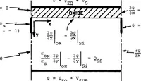
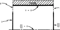
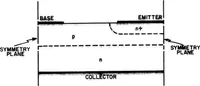
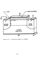
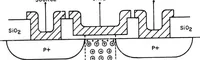
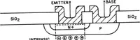
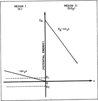
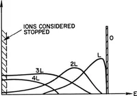
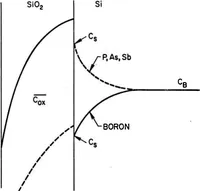
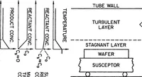
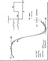
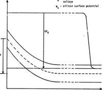
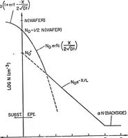
A 1976 technical report on computer-aided engineering of semiconductor integrated circuits, issued by the Defense Technical Information Center for engineers and researchers working on device design. Its figures are plain engineering line drawings and graphs: boundary-condition sketches of an oxide layer over silicon, a graph of carrier concentration plotted against depth, and a cross-section of an isolated transistor structure with source, gate and P+ diffusion regions. A designer could take their clean schematic style, with labelled arrows, dashed boundary lines and hatched oxide fills, as a model for technical diagrams.